
DDR2 Memory Controller User's Guide

www.ti.com
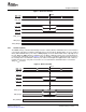
DDR2 memory controller data bus
DDR_D[31:24]
(Byte Lane 3)
DDR_D[23:16]
(Byte Lane 2)
DDR_D[15:8]
(Byte Lane 1)
DDR_D[7:0]
(Byte Lane 0)
32-bit memory device
16-bit memory device
2.6 Address Mapping
Peripheral Architecture
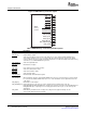
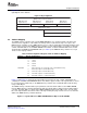
Figure 10 shows the byte lanes used on the DDR2 memory controller. The external memory is always
right aligned on the data bus.
Figure 10. Byte Alignment
The DDR2 memory controller views external DDR2 SDRAM as one continuous block of memory. This
statement is true regardless of the number of memory devices located on the chip select space. The
DDR2 memory controller receives DDR2 memory access requests along with a 32-bit logical address from
the rest of the system. In turn, DDR2 memory controller uses the logical address to generate a row/page,
column, and bank address for the DDR2 SDRAM. The number of column and bank address bits used is
determined by the IBANK and PAGESIZE fields (see Table 5 ). The DDR2 memory controller uses up to
14 bits for the row/page address.
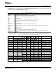
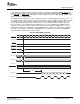
Table 5. Bank Configuration Register Fields for Address Mapping
Bit Field Bit Value Bit Description
IBANK Defines the number of internal banks on the external DDR2 memory.
0 1 bank
1h 2 banks
2h 4 banks
3h 8 banks
PAGESIZE Defines the page size of each page of the external DDR2 memory.
0 256 words (requires 8 column address bits)
1h 512 words (requires 9 column address bits)
2h 1024 words (requires 10 column address bits)
3h 2048 words (requires 11 column address bits)
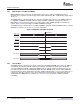
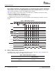
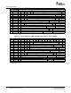
Figure 11 and Figure 12 show how the logical address bits map to the row, column, and bank bits all
combinations of IBANK and PAGESIZE values. Note that the upper four bits of the logical address cannot
be used for memory addressing, as the DDR2 memory controller has a maximum addressable memory
range of 256 Mbytes.
The DDR2 memory controller address pins provide the row and column address to the DDR2 SDRAM,
thus the DDR2 memory controller appropriately shifts the logical address during row and column address
selection. The bank address is driven to the DDR2 SDRAM using the bank address pins. The two lower
bits of the logical address decode the value of the byte enable pins (only used for accesses less than the
width of the DDR2 memory controller data bus).
Figure 11. Logical Address-to-DDR2 SDRAM Address Map for 32-Bit SDRAM
SPRUF85 – October 2007 DSP DDR2 Memory Controller 19
Submit Documentation Feedback