
Computer Hardware User's Guide


www.ti.com
1.3 Printed Circuit Board Assembly
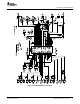
1.4 USB to I
2
C Interface Board (EV2300)
1.5 Software
2 Setup
2.1 Input / Output Connector Descriptions
Setup
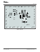
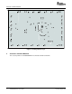
The TPS65020EVM-110 PCB contains the TPS65020 IC and its required external components. This
board contains several jumpers and connectors that allow the user to customize the board for specific
operating conditions.
The EV2300 is the link that allows the PC and the EVM to communicate. One end of the EV2300
connects to the PC with the supplied USB cable, and the other end of the EV2300 connects to the EVM
with the supplied Molex cable. When the user writes a command to the EVM, the interface program, which
is run from the PC, sends the command to the PC USB port. The EV2300 receives the USB command
and converts the signal to an I
2
C protocol. It then sends the I
2
C signal to the TPS65020 board. When the
user reads a status register from the EVM, the PC sends a command to read a register on the EVM.
When the EVM receives the command, it reports the status of the register via the I
2
C interface. The
EV2300 receives the information on the I
2
C interface, converts it to a USB protocol, and sends it to the
PC.
Texas Instruments has provided software to assist the user in evaluating this EVM. To install the software,
insert the enclosed CD into your computer. The software should start automatically. If it does not, simply
go to <Start>, <Run>, and type “D:\SLVU138.exe”, and click <OK> (assuming that D: is your CD drive).
The program should run without errors. If any problems occur that result in the program not being
installed, view the readme.txt file on the CD for further information. Check the TPS65020 product folder on
the TI website for the latest revision of the software.
This section describes the jumpers and connectors on the EVM as well as how to properly connect, setup,
and use the TPS65020EVM-110.
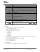
INPUT / OUTPUT DESCRIPTION
Input voltage from external power supply, recommended maximum 5.5 V. Input current is dependent
J1 – VIN
on load but is typically below 2 A.
J2 – GND This is the return connection for V
I
.
Input voltage and return for LDO1 and LDO2C. Resistor R23 connects this pin to VDCDC1. If an
J3 – VINLDO/GND
external power supply is used, remove R23. Recommended maximum input voltage is 5.5 V
Input voltage and return for VSYSIN, one of the input voltages for RTC. Resistor R24 connects this
J4 – VSYSIN/GND input to VDCDC1. If an external power supply is used, remove R24. Recommended maximum input
voltage is 4 V
Input voltage and return for VBACKUP, one of the input voltages for RTC. There is no on board
J5 – VBACKUP/GND
connections to a voltage input. Recommended maximum input voltage is 4 V.
Direct connection to the GPIO1 and GPIO2 pins. For this EVM, GPIO1 is configured as a
J6 – GPIO1/GPIO2
push-button input, and GPIO2 is configured as an LED output.
J7 – VRTC/GND Output voltage from the RTC circuit.
Four fault outputs are available on this connector:
PWRFAIL - Fault occurs when input voltage is below 3 V. Pulled up to VRTC when safe, low for fail.
INT - Fault occurs when there is a fail on an input or output voltage. It acts as a sum fail. Pulled up
J8 – Fault Outputs
to V
I
when safe, low for fail.
RESPWRON– Low reset signal controlled by SW2, 300 mS. Pulled up to V
I
normally.
LOWBAT– Fault occurs when input voltage is below 3.6 V. Pulled up to V
I
when safe, low for fail.
J9 – USB This header duplicates the signals from the J20 interface connector.
Output from DCDC1 switching regulator, maximum output current is 1.2 A, default voltage setting is
J10 – VDCDC1
3.3 V.
TPS65020EVM-110 User's Guide2 SLVU138 – August 2005