
Digital Amplifier User's Guide

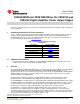
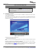
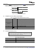

Outputstagepowersupply
RESET
>1ms
Systempowersupply
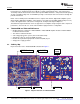
4.2 J1 Amplifier Connection to MC012 Controller Module
4.3 Loudspeaker Connectors (J3 - J6)
System Interfaces
www.ti.com
The recommended TAS5102/3 power-up sequence is shown in Figure 4 . For proper TAS5102/3
operation, the RESET signal should be kept low during power up. RESET is pulled low during power up
for 200 ms by the onboard reset generator (U2).
Figure 4. Recommended Power-Up Sequence
Table 4. J9/J10 Pin Description Amplifier/Controller Connector
Net-Name at
Pin No. Description
Schematics
1, 2, 5, 6 ,10, 11, 28 DGND Low-current ground for modulator/controller
3, 4 PVDD1 PVDD buffered through 24- Ω resistor to power the modulator/controller
7 OTW Overtemperature warning from the amplifier (T > 125 ° C)
8, 9, 13, 15, 17, 19, 20, 21,
NC Not connected
22, 23, 25, 27
12 PWM_A Channel A PWM signal from modulator
14 PWM_B Channel B PWM signal from modulator
16 PWM_C Channel C PWM signal from modulator
18 PWM_D Channel D PWM signal from modulator
24 RESET Resets the TAS5102/3
26 FAULT Power stage fault indicator
CAUTION
Both positive and negative speaker outputs are floating and may not be
connected to ground (e.g., through an oscilloscope).
Table 5. Output Pin Description
Net-Name at Schematics Description
OUT_A Speaker positive output
OUT_B Speaker negative output
OUT_C Speaker positive output
OUT_D Speaker negative output
TAS5102EVM and TAS5103EVM for the TAS5102 and TAS5103 Digital Amplifier Power Output Stages10 SLLU106 – August 2008
Submit Documentation Feedback